
It’s fun to build electronics circuits.
Regulated DC Power Supply
When making various things necessary for amateur radio, or electronics tests, we sometimes need an adjustable DC power supply. Various power supplies are sold in the market, but they are expensive, especially ones whose output is continuously variable from 0 V to 16 V DC. This time, I decided to build it by myself. The circuit should be as simple as possible, easy to make and use no special components.

1. Circuit design
There are two types of regulated DC power supply systems. One uses a switching voltage regulator and the other uses a linear voltage regulator. The regulated DC power supply in this plan is the type that basically does not generate noises from its circuit and its output is only 3 amps.
I decided to design a power supply that outputs 0 to +15 V continuously, with a current capacity of around 3A. If the power supply needs to output 0 V, you need to add a special circuit, and I decided to use a minus (negative) voltage to achieve the specification.
Normally, we use a transformer to convert the AC line voltage to a lower AC voltage, which is then rectified and regulated by the voltage regulator circuit. This time, I needed to think of a variety of AC input voltages that are used in various readers’ countries. Therefore, I used an AC adapter with a universal input, and outputs 18 V DC at 3 A or more. I had a little concern about the noise that is generated, because it is a switching power supply. However, the main power supply circuit is not the switching regulator type, and I thought the noise could be decreased.
The circuit design is shown below.
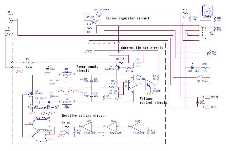
The voltage control circuit in this power supply is built with an Op-amp (IC3A). A positive and a negative 5 V are applied to the IC for its operation. As the noninverting (+) input terminal of IC3A is connected to the ground, the inverting (-) input terminal voltage is controlled going close to 0 V. An output voltage is applied to one terminal of potentiometer R20, and the other terminal is connected to 5 V through R1 (3.3 kΩ). As the center terminal of potentiometer R20 is connected to the inverting input terminal of the Op-amp through R2 (10 kΩ), the terminal goes close to 0 V when the R20 is rotated to the R1 side, and the voltage at the other end of the terminal becomes 15 V, as shown in the diagram below. Therefore, I know that the maximum output voltage is 15 V. The sum of the resistance values for R1 (3.3 kΩ) and R20 (10 kΩ) is 13.3 kΩ, and half of it is 6.65 kΩ, as you can see. The output voltage of this power supply will be 5 V at this 6.65 kΩ point.
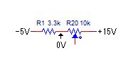
Fig. 2
I planned to build the power supply with a current capacity of approximately 3A. I used a 2SC5199 NPN transistor (Q1), as I had some in my drawer. This transistor has more current capacity, 12 A maximum collector current. A transistor for a smaller current capacity can also be used with no problem. I also used a JA7151 PNP type transistor for as I had some on hand, but there is no special reason to use them. If you prefer to use a 2SB type transistor (PNP type), you can use 2SB1182 or 2SB1240. These two NPN and PNP transistors are connected in a Darlington pair configuration.
Digital transistor DTC114 is used as a buffer of the OP amp. The transistor has two resistors in its package, as shown in the circuit diagram below. If you cannot get such a digital transistor, you can just use a regular transistor and connect two external resistors to the transistor. When the output voltage of IC3A is somehow increased, the transistor current becomes larger and the current flow of the Darlington connection consisting of Q1 and Q2 is also increased for toward increasing output voltage.
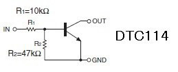
Fig. 3 Internal connections of the digital transistor
Here is the explanation of producing the negative voltage circuit.
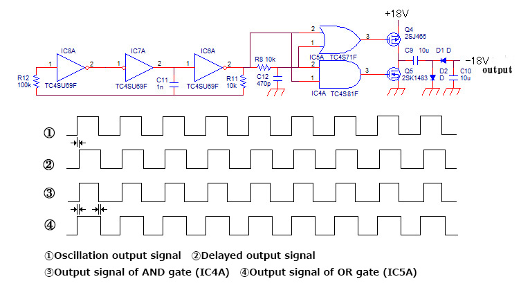
Fig. 4 Output signals at each point
IC6 to IC8 make an oscillator by a 3-step inverter, and it oscillates at approximately 47 kHz. The oscillator output signal drives FETs for direct switching. However, the output signals of IC4A need to be waveform-shaped because PMOS and NMOS FETs may simultaneously turn ON without waveform-shaping. If both FETs are simultaneously turned ON, the circuit will short out, and that must be avoided.
Therefore, the oscillator output signals produced by IC6A, IC7A, and IC8A are delayed by an integrating circuit consisting of R8 and C12. The signal is then applied to IC4A and IC5A, an AND gate and an OR gate respectively, to drive the FETs. This function does not make the FETs simultaneously turn ON.
To produce a negative voltage power supply, it is easy if you replace the FETs with mechanical switches, as in an equivalent circuit, shown in the diagram below.
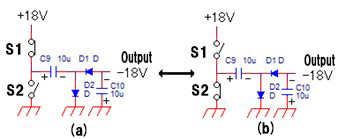
Fig. 5 Switching analysis in the equivalent circuits
As shown in Fig. 5(a), when S1 is ON (closed position), current flows from the +18 V line to D2 through C9. Then, C9 is charged. In the next cycle, S1 and S2 are in the positions in the diagram shown in Fig. 5(b), and the hot end of C9 is connected to ground. Then, C10 is charged through D1.
It is possible to get output of -18 V by repeating this cycle.
The Series Voltage Regulator (IC2) provides the -5V that is supplied to the Op-amp. This circuit may be suitable for studying the theory of power supply circuits, but it requires many components. However, if you use the LM2662 or LTC1144, it may be easier to build the 5 V power supply circuit with fewer components needed.

Fig. 6 ±5 V power supply circuit
To avoid damaging the power supply circuit if the output terminals are accidentally shorted, a current limiter circuit is included. The circuit is shown in Fig. 7 below.

Fig. 7 A current limiter circuit
When current flows in the output terminals, a voltage drop occurs on R4. As the current increases, the base-emitter voltage also increases. When the voltage becomes 0.5 V, the collector current starts to flow. The current is applied to IC3A (Op-amp) through R3 to reduce the voltage, and the circuit is protected from the large amount of current flow at the output terminals.
The power supply has a meter showing the output voltage and the amount of current. I use a 1 mA current meter for both voltage and current meters. I made the meter indication panel with card board, as shown in Fig. 8. The full-scale readings for voltage and current are 20 V and 5 A, respectively.

Fig. 8 The meter indication panel
The internal resistance of the ammeter I used is 100Ω. The meter circuit was designed using an ammeter. As readers have different meter needs, depending on your situation, I skipped the explanation of this circuit. You can use independent meters for voltage and amperage.
Here are examples of shunts and multipliers if you use the same ammeter I used.
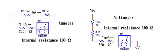
(left) Fig. 9 Shunts for the ammeter
(right) Fig. 10 Multipliers for the voltmeter
2. Assembly
I am concerned about desk space, so that I decided to design the power supply in a vertical configuration. If you are not concerned about space, you can select any case style you like.
The meter I used was an ammeter with a 1 mA full-scale deflection, (100 Ω internal resistance), because I had it in my parts drawer. Even you have the same full-scale ammeter, the internal resistance may not be the same as the one I used. You should calculate shunts and multipliers using the formula we learned when we took the test for our license. I do not use special components so that it may be easy to get them at a parts store.
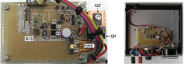
(left) Fig. 11 Print circuit board (right) Fig. 12 Inside view
As the power supply has a current limiter circuit installed, I don’t have to worry about overcurrent flow. However, to protect it from any damages, I put in a fuse for extra protection. The fuse I installed is one for motor vehicles. See the picture in Fig. 11.
Q1 and Q2 should be placed close together for easy wiring. As a large amount of current flows through Q1, you should mount it on an aluminum plate (heatsink). The collector on Q1 is not insulated. When you mount Q1, place a mica insulator between it and the aluminum plate. For better heat dissipation, use a thermal compound between the collector (transistor case) and the aluminum plate. See the manufacturer’s specification sheet attached, for lead allocations.

Fig. 13 Thermal compound and the mica insulator
The power source is an AC adapter for my desktop computer. As I mentioned in the beginning, the output voltage is 18 V DC and the current capacity is 3 A. The power supply I designed this time has 15 V maximum, so your power source must have an output voltage of 18 V or more.

Fig. 14 AC adapter
If you do not have a similar AC adapter for a power source, you can build a power source with the following discrete components.
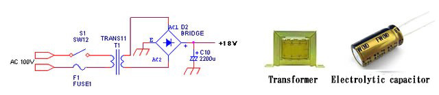
Fig. 15 Power source schematic diagram using a transformer
It may be convenient if you have such a variable output voltage DC power supply. I use it for a variety of experiments, and for my mini-drill.

