


Technical Trivia by Dr. FB
The principle of PLL
Learn the basic of PLL technology again.
Dr. FB
A Signal Generator (SG) is useful for small electronic work and radio adjustment. If you only want the generator part of SG, recently you can buy a PCB unit relatively cheaply, but the problem is the attenuator that can fine-tune the signal level. That is expensive. I wanted a signal generator for testing radios, and while thinking about making it, I came up with the principle of PLL (Phase Locked Loop).
Let’s try to solve a problem of a simple PLL circuit
First, let's solve a simple PLL problem. For reference, this problem is the same as the one given on the national examination test for the Japanese first-class amateur radio license.
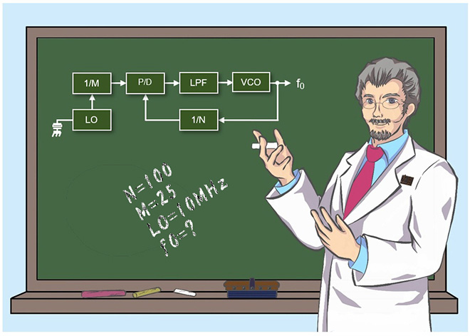
【Problem】
In the frequency synthesizer oscillator shown in Figure 1 below, there is a PLL circuit with the following conditions. Find the output frequency fo when the frequency division ratio (N) of the programmable divider is 100. However, it is assumed that the output frequency of the reference oscillator is 10 MHz, the frequency division ratio of the fixed divider is 25, and the PLL is locked.
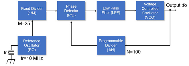
Figure 1. PLL Block Diagram

Background of PLL
Before explaining the principle of PLL, I will briefly explain first a transceiver using a crystal unit, and then second give an overview of PLL. After that, I will explain each block.
(1) A transceiver using a crystal unit
Figure 2 shows Icom's IC-212, 144 MHz 15-channel FM portable transceiver released in 1976.

Figure 2. IC-212 144 MHz 15-Channel FM portable transceiver
When you open the case, you can see the sockets that hold crystals for one of the 15 channels surrounded by the yellow dotted lines, in Figure 2 (b). Figure 2 (c) is an enlarged view of it. Each of the 15 channels requires a separate crystal for transmission and reception, and if you install 15 channels, you will need 30 crystals.
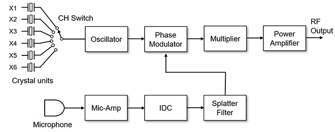
Figure 3. Block diagram of a 6-channel FM transceiver
X1 to X6 in Figure 3 are crystal units. Now, when you buy a transceiver, you can transmit and receive on any frequency in the band by turning the channel switch. When the above IC-212 was released, it was necessary to insert one pair of crystal units of the desired frequency into the radio to transmit and receive on the channels.
For example, in the 2-meter band, there are 50 channels with 20 kHz spacing for the FM mode from 145.00 MHz to 145.98 MHz in Japan. If you want to operate on all the channels, you would 100 crystals, 50 for transmit and 50 for receive. Since the crystal unit also has a physical size, if you try to insert all 100 crystal units into the radio would require a large physical space. In that case, the radio will become very large. Inevitably, the question is whether to choose the size or the number of channels.
(2) Is VFO useless?
You can make an oscillation circuit called a VFO (Variable Frequency Oscillator) with a coil (L) and a capacitor (C) without using crystal units. The VFO can replace the crystal units and produce a signal with a continuously adjustable frequency. So, if you use the signal from a VFO in the local oscillator circuit, you can transmit and receive on any frequency.
However, since the circuit is an oscillator composed of L and C, it is greatly affected by external vibration, ambient temperature, and humidity, and it is quite difficult to maintain frequency stability in a communication device. The crystal unit also causes frequency fluctuations due to external factors, but the frequency stability is outstanding compared to the frequency fluctuations of VFOs.
It was stated in a book about the theory of PLL, that PLL was already used for frequency control in generators at the beginning of the 20th century. PLL began to be used in the field of communications equipment after radio broadcasting began in the 1920s. I think that it the cost and space required to build circuits using vacuum tubes was too much at that time to introduce it to consumer equipment.
A PLL does not use special parts like a VFO. The only special thing is how to control the stability of the frequency. The VFO compensated for temperature changes by using a component that cancels the temperature change and stabilized the frequency. In a PLL, the frequency is stabilized by a circuit that is always electrically automatically controlled to match the stability of the crystal unit.
Overview of the PLL
(1) Block diagram of PLL circuit
The PLL is a kind of feedback circuit. As shown in Figure 4, the basic circuits of the PLL consist of a Reference Frequency Oscillator, a Fixed Divider, a Phase Detector, a Low Pass Filter (LPF), a VCO (Voltage Controlled Oscillator) and a Programmable Divider.
You can use the signal oscillated by an oscillator consisting of L and C circuits, such as a local oscillation signal in a radio, but the frequency stability is very poor and stable communication cannot be made.
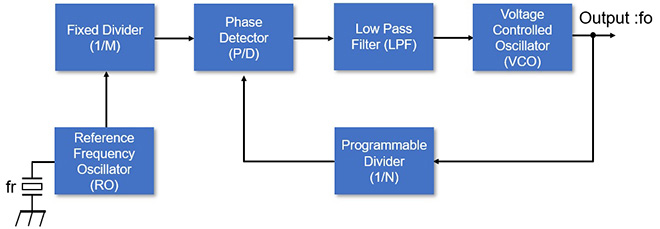
Figure 4. Principle diagram of PLL used for communication equipment
That is where the PLL shown in Figure 4 comes into play. The phase detector compares the two signals, signal (fr) oscillated by the reference frequency oscillator and signal (fo) oscillated by the VCO. The oscillation frequency of the VCO is controlled and stabilized by using the output voltage according to the phase difference between these two signals. For example, if the output voltage of the phase detector is high, the oscillation frequency is lowered, and vice versa. The control method will be explained in a little more detail in the VCO described later.
(2) Fixed frequency divider (1/M)
This is a circuit that reduces the input frequency to a fraction of an integer. In most cases, a dedicated IC for frequency division is used. In the problem shown at the beginning, M=25. In other words, it is a circuit that outputs the input 10 MHz signal to 1/25, that is, 400 kHz.
(3) Programmable divider (1/N)
This is also known as a programmable divider. Any division ratio can be set with external terminals. In combination with the CPU, turning the dial of the radio changes the frequency division ratio, and the frequency of the signal output from the programmable frequency divider (1/N) can be changed.
(4) Phase Detector
The phase detector compares the phases of two signals and responds to the phase difference. In other words, phase comparison means frequency comparison. One signal (fr) input to the phase comparator has outstanding stability because it is originally an oscillation of a crystal unit. If the signal (fo) of another VCO exactly matches that frequency, the two sine waves in Figure 5 will overlap and there will be no phase difference. In other words, the two frequencies match.
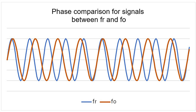
Figure 5. Phase comparison of fr and fo
It seems that there are various types of phase detectors, but for example, in the old method, there is also a phase detector that takes the beat frequency of the fr and fo signals and outputs the voltage, depending on beat frequency. In other words, it is f-V (Frequency – Voltage) conversion. When the beat frequency is 0, the output voltage of the phase detector is 0 (V). When a beat is generated, the voltage corresponding to it is output.
Figure 6 shows a part of the PLL circuit used in Icom's IC-2A series transceiver (released in 1980). IC2 (TC5081) is an IC of the phase comparator. It seems that this IC has already been discontinued and only distribution stock remains, but it is an easy-to-use IC for homebrewers.
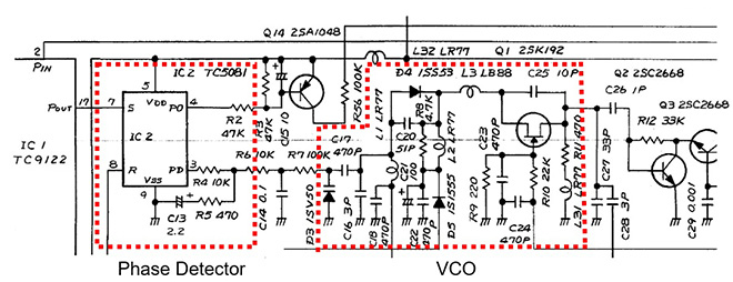
Figure 6. IC-2A series phase detector and circuit around VCO (excerpt from Icom IC-2A circuit diagram)
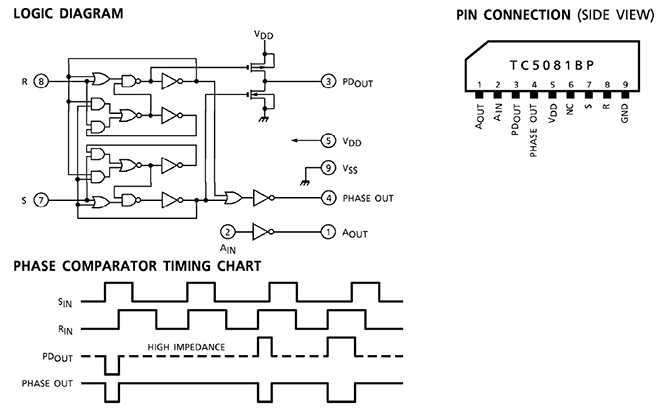
Figure 7. Internal circuit of phase comparator IC used for IC-2A series and its timing chart (Quoted from the data sheet of TOSHIBA TC5081)
(5) Low Pass Filter
Also known as a Loop Filter. The schematic in Figure 6 consists of R4, R5, R6, C13 and C14. Since the output of the phase detector contains noise and high frequency components, they are removed to create a DC component signal to be supplied to the D3 (Varactor diode) of the VCO.
(6) Voltage Controlled Oscillator (VCO)
The circuit consisting of Q1 (2SK192) in Figure 6 and its peripheral circuits is the VCO (Voltage Controlled Oscillator) circuit. The key component of the Colpitts oscillator is a D3 (1SV50) varactor diode.
I mentioned that the VCO is an oscillator circuit consisting of L and C, but the key point is that a varactor diode is used in some of its circuits. A varactor diode is a type of diode, but it has the characteristic that the capacitance between the anode and cathode changes when a voltage is applied in the opposite direction. In other words, the C (capacitance) of this varactor diode is used in the LC oscillation circuit, and the VCO oscillation frequency is changed by changing the capacitance of this C.
When a phase difference occurs in two signals between fr and fo compared by the phase detector, the voltage output from the phase detector is large when the phase difference is large, and the voltage is low when the phase difference is low. By applying that voltage to the varactor diode in the VCO circuit, the PLL changes the oscillation frequency of the VCO so that it becomes the same frequency as the reference frequency (fr).
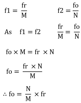
Relationship between fr and fo
Let f1 be the frequency obtained by dividing the signal oscillated by the reference frequency oscillator (RO) with the fixed frequency divider (1/M). Also, let f2 be the frequency obtained by dividing the VCO output signal (fo) with the programmable divider (1/N). PLL is an automatic control circuit with a kind of feedback that makes the relationship between f1 and f2 for f1=f2. When f1=f2, we say "PLL is locked." On the other hand, if f1=f2 is not set for some reason, it is said that the PLL is in the unlocked state.
The reference frequency oscillator (RO) frequency is fr in Figure 8. Since the frequency of fr is a high frequency on the order of MHz, it is divided by a frequency divider (1/M) to make it a lower frequency. The output frequency f1 of the divided fixed frequency divider is f1=fr/M. Design the VCO oscillation frequency in advance in the LC circuit as the desired target frequency. The desired target frequency fo is a signal used in the local oscillator circuit (LO) of the radio circuit, so turning the dial of the radio changes the frequency. Therefore, the frequency division ratio is determined so that the variable frequency divider (1/N) is constantly programmed from the outside to have a frequency of f1. In other words, f2 is the VCO output frequency (fo) divided by N, so f2 = fo/N.
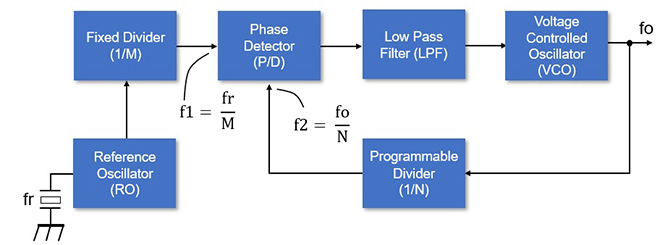
Figure 8. Relationship between fo and the divided ratio (N/M)
IC-2A/AT PLL circuit
The IC-2A/AT PLL circuit uses a fr = 5.12 MHz crystal unit. The 5.12 MHz is divided by 1024 with a fixed frequency divider (1/M), and the 5 kHz signal is input to the phase detector as f1. The other signal, f2, enters the phase detector and divides the output frequency of the VCO to obtain 5 kHz. Here, since M and fr are constant, it can be understood that the output frequency (fo) of the VCO changes by changing the division ratio N.
IC-221 PLL unit
The IC-221 was launched in 1976. Figure 9 shows the PLL and VCO units of the IC-221 (IC-211 for the export model name). As you can see the large LSI (SC3062A) in the PLL unit. This is a PLL IC. This IC contains circuits with functions such as a fixed divider, programmable divider, and phase detector etc.
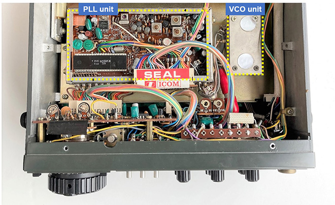
Figure 9. IC-211 PLL and VCO units
FBDX
<Reference material>
Japan Radio Institute, Question pool for the 1st class amateur radio examination in April 2017
TOSHIBA, TC5081 Data sheet
Icom Incorporated, IC-2A/AT circuit diagram
Technical Trivia by Dr. FB backnumber
- Generating “Sawtooth Waves” using a D/A conversion circuit and a counter IC
- Examining a D/A converter using a Resistor Ladder
- Electronic firefly and its circuit description
- Controlling the rotation speed of a DC motor
- Description of up-down counter using 74HC192 and 74HC4511 ICs
- Considerations when making a dual voltage power supply for operational amplifiers
- Observing filter characteristics with a white noise generator
- Is noise actually reduced in twisted pair cables?
- Experiments on divider circuits using a 74HC74
- Consideration of using a photocoupler as a voltage-variable resistor
- Distorted waveform spectrum as observed on a tinySA
- Trial making of a QFH antenna
- About the inductance of coils
- Operation of analog switches
- Small digital voltmeter, 2-wire type / 3-wire type. What is the difference?
- Constant current circuit using an Op-Amp
- Coaxial cable loss to UHF and SHF
- 2.4 GHz Wireless LAN Antenna
- Let’s use MOSFETS
- 25th Comparator
- The principle of PLL
- Examination of the MLA performance
- About the Fresnel zone of the SHF band
- Level difference under open and load ends of an SSG
- Is “Made in Japan” alive? (UHF adapter again)
- Possibility experiment of passive repeater with the Back-to-Back antenna
- Why you should make SWR measurements just below the antenna!
- How reliable is the L-type BNC?
- Is the Bird 43 accurate enough?
- Does a wire dipole antenna need a balun?
- Why we don’t use a silicon diode in a crystal radio?
- How to light the 7-segment LED
- Measurement of Antenna Performance on Handheld Transceivers (Part 3)
- Measurement of Antenna SWR on Handheld transceivers (Part 2)
- Measurement of Antenna SWR on Handheld transceivers(Part 1)
- An SWR meter
- V/UHF 3-Band Antenna Dismantling Note