


Technical Trivia by Dr. FB
Let’s use MOSFETS
Understanding the switching function of MOSFET transistors

Dr. FB
MOSFETs are often used for switching circuits. They function by applying a voltage, without passing large current as with mechanical replays. Here I will explain the switching operation, which is a major feature of MOSFETs.
What is a MOSFET?
A MOSFET is a type of transistor. Transistors are roughly classified as FETs. As you know, FET is an abbreviation of Field Effect Transistor. The MOS in front of FET is an abbreviation for Metal Oxide Semiconductor. This is a name derived from the semiconductor structure of an FET, but the structure is skipped because Dr. FB is not good at semiconductor structure.
Since it is an FET, it is not a current driven element that controls the collector current by changing the base current as in a normal bipolar transistor. Since the current between the drain and source is controlled by the gate-source voltage (VGS), it can be said that it is a voltage driven element. A voltage is applied to each lead-wire of the MOSFET, but the structure does not allow current to flow through them, which is very useful for energy-saving circuits.
Due to the structure of MOSFETs, there are two types of FET, as shown in Figure 1. One is an N-channel MOSFET and the other is a P-channel MOSFET. In terms of operation, there are two types of MOSFET: the depletion type, which is often used for high-frequency amplification circuit, and the enhancement type, which is used in switching circuits. This article is limited to the latter enhancement type MOSFET.
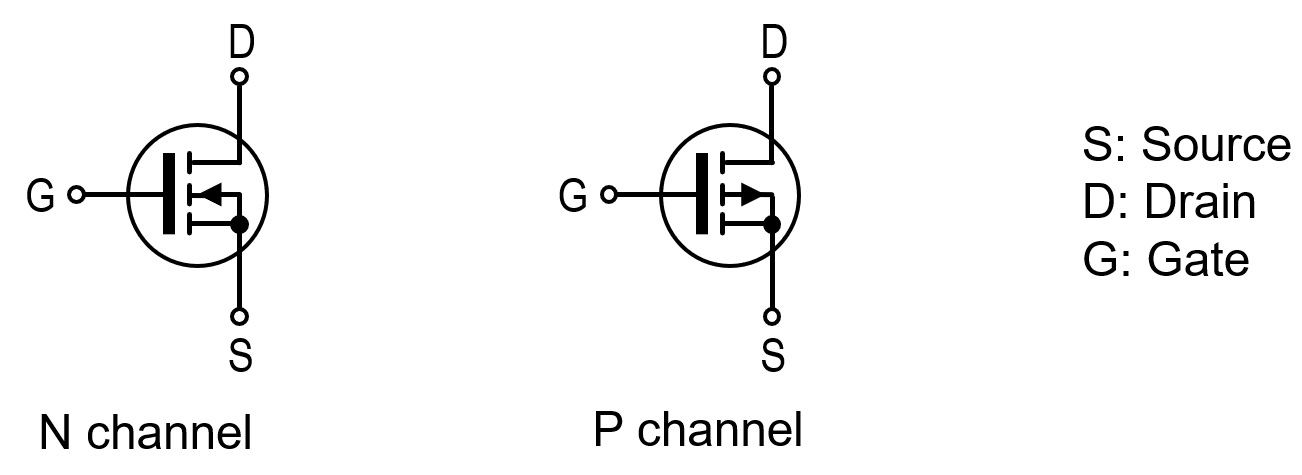
Figure 1. Enhancement MOSFET schematic symbols
The resistance value (RDS) between the drain and source changes, depending on how the voltage (VGS) between the gate (G) and source (S) of the MOSFET is applied. This issue of Short Break features an article on electronic circuit using P-channel MOSFETs. This utilizes the fact that the voltage applied to the gate is (+) voltage or the same potential with respect to the source, so that the drain and source are turned OFF.
Basic operation of MOSFETs
If you understand the basic switching operation of MOSFETs, you can turn electronic circuits ON or OFF that were previously turned ON or OFF with mechanical relays. With MOSFETs you can save energy as well as digitize the circuits.
(1) Gate (G) - source (S) voltage vs. drain current
When the voltage (VGS) between the gate (G) and the source (S) of the N-channel MOSFET is 0 (zero), the drain current (ID) does not flow. When the voltage (VGS) is gradually increased, the resistance value (RDS) between the drain (D) and source (S) begins to decrease, and the drain current begins to flow. In order to lower the resistance value sufficiently, it turns ON. It is necessary to raise VGS sufficiently. By setting the voltage above the threshold voltage (VTH) in the manufacturer's data sheet, the RDS will decrease, and it will function as a switch.
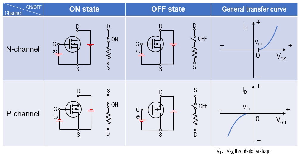
Figure 2. ON/OFF operation vs. VGS and characteristic curves
(2) Switching time
Switching by a mechanical relay is controlled with a transistor, as shown in Figure 3. When a voltage is applied to the base, the base current (IB) flows and the transistor used for switching turns ON. When the transistor turns ON, a current flow through the drive coil of the relay, which becomes an electromagnet, and the contact of the relay makes a click sound and connects to another contact. At this time, the contacts are switched mechanically, which causes a physical time delay. It takes less than 10 milliseconds for small mechanical relays, but it seems that it takes several tens of milliseconds for large relays.
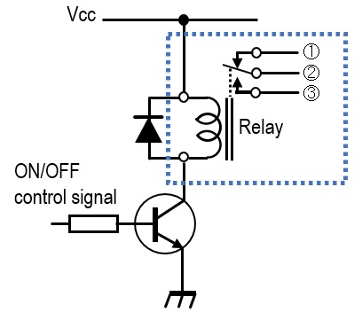
Figure 3. Mechanical relay drive circuit by a transistor
According to the 2SJ555 data sheet published by Renesas Electronics Corporation, the turn ON/OFF delay time is in the nanoseconds. In other words, since it is 10 to the power of minus 9, it can be seen that it is incomparable to the millisecond order of mechanical relays.
(3) Resistance (RDS) between drain (D) and source (S)
The data sheet mentioned above shows the ON-resistance value (RDS) when the MOSFET is operating as a switch. If the MOSFET operates as a switch, the ON-resistance value (RDS) between the drain and source that replaces the relay contacts is very important. The data sheet states that RDS is 0.017 Ω when VGS = -10 V and ID = -30 A. 0.017 Ω is a fairly low value. Assuming that this MOSFET switches the current of 20 A that flows when a 100 W radio is connected, the power consumed by RDS is P = 20 x 20 x 0.017 = 6.8 W from P = I2 x R. You will need a small heatsink, but I don't think it is enough heat to cool with just a fan.
(4) Specific example of VGS vs. RDS
Figure 4 shows the principle of turning the P-channel MOSFET ON or OFF with the gate voltage. When the SW is ON (switch is closed), the gate is connected to ground through the switch, so the gate voltage becomes zero. As a result, the drain-source resistance (RDS) becomes low and comes close to conduction. Conversely, when the SW is turned OFF (switch is open), same voltage as the source is applied to the gate through the resistor (R). The P-channel MOSFET is turned OFF and no current flows between the source and drain.
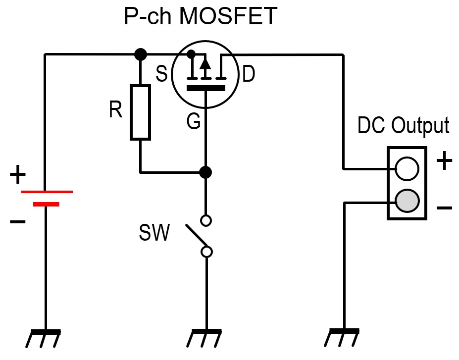
Figure 4. Principle diagram of switch using P-channel MOSFET
The overvoltage protection device built by replacing the switch in Figure 4 with a transistor is published in this issue of Short Break.
CL
Technical Trivia by Dr. FB backnumber
- Generating “Sawtooth Waves” using a D/A conversion circuit and a counter IC
- Examining a D/A converter using a Resistor Ladder
- Electronic firefly and its circuit description
- Controlling the rotation speed of a DC motor
- Description of up-down counter using 74HC192 and 74HC4511 ICs
- Considerations when making a dual voltage power supply for operational amplifiers
- Observing filter characteristics with a white noise generator
- Is noise actually reduced in twisted pair cables?
- Experiments on divider circuits using a 74HC74
- Consideration of using a photocoupler as a voltage-variable resistor
- Distorted waveform spectrum as observed on a tinySA
- Trial making of a QFH antenna
- About the inductance of coils
- Operation of analog switches
- Small digital voltmeter, 2-wire type / 3-wire type. What is the difference?
- Constant current circuit using an Op-Amp
- Coaxial cable loss to UHF and SHF
- 2.4 GHz Wireless LAN Antenna
- Let’s use MOSFETS
- 25th Comparator
- The principle of PLL
- Examination of the MLA performance
- About the Fresnel zone of the SHF band
- Level difference under open and load ends of an SSG
- Is “Made in Japan” alive? (UHF adapter again)
- Possibility experiment of passive repeater with the Back-to-Back antenna
- Why you should make SWR measurements just below the antenna!
- How reliable is the L-type BNC?
- Is the Bird 43 accurate enough?
- Does a wire dipole antenna need a balun?
- Why we don’t use a silicon diode in a crystal radio?
- How to light the 7-segment LED
- Measurement of Antenna Performance on Handheld Transceivers (Part 3)
- Measurement of Antenna SWR on Handheld transceivers (Part 2)
- Measurement of Antenna SWR on Handheld transceivers(Part 1)
- An SWR meter
- V/UHF 3-Band Antenna Dismantling Note