


Technical Trivia by Dr. FB
Constant current circuit using an Op-Amp
Dr. FB
An article "Building a 20 Amp electronic DC load device using an N-channel MOSFET for the load” is published in the October issue of FB NEWS. An operational amplifier is used in the device for keeping the same current flow. The circuit is to enable a constant current to flow even if the voltage changes. According to Ohm's law, the current changes when the voltage changes, but by incorporating this circuit, the flowing current can be kept constant. There are various types of circuits that make up the constant current, but this time I will briefly explain it that uses an operational amplifier.
Drain current (ID) control
Figure 1 shows the circuit that controls the ID of the enhancement type MOSFET. In this circuit, the power supply voltage VCC is constant, and the VGS voltage is changed with R2 to control the ID. However, VCC may fluctuate for some reason. When VCC fluctuates, ID also fluctuates. A constant current circuit constantly monitors the ID and tries to make the ID electronically constant. The circuit in Figure 1 uses an N-channel MOSFET. The enhancement type of the N-channel MOSFET changes the ID according to the magnitude of VGS when VGS becomes a positive voltage, as shown in the graph below.
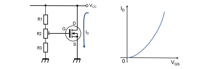
Figure 1. VGS vs. ID characteristics
Constant current circuit using operational amplifier
Figure 2 shows the circuit diagram of the 20A electronic DC load device. The red highlighted part makes up the constant current circuit.
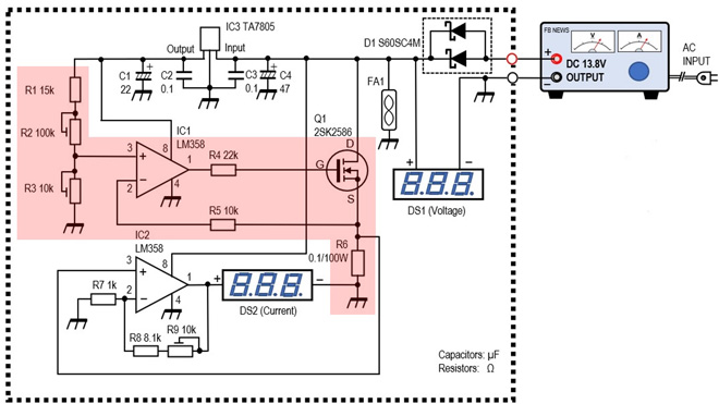
Figure 2. Circuit diagram of the 20A electronic DC load device
About the “Imaginary short circuit” of the operational amplifier
In order to understand the constant current circuit using an operational amplifier, it is essential to understand the basic operation of the operational amplifier. Since an operational amplifier is called an "amplifier," the component itself is a device that amplifies signals. The open gain that an operational amplifier has is very high, about 100 dB (10 to the 5th power). However, inputting a voltage of 1 V does not mean that the output will be a voltage of a hundred thousand of volts amplified by 100 dB. The output does not exceed the power supply voltage. Operational amplifiers are usually used with stable gain by applying negative feedback, as shown in Figure 3.
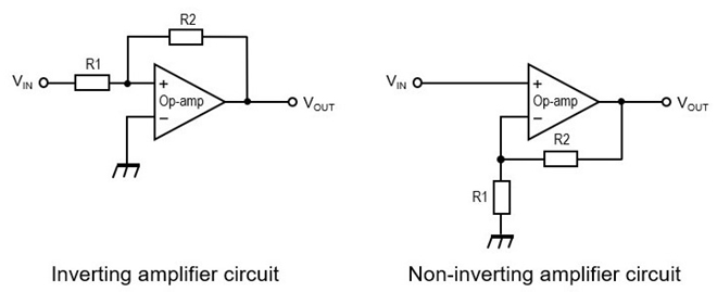
Figure 3. Basic diagrams of negative feedback in operational amplifier circuits
Operational amplifiers have (+) and (-) input terminals. The former is called the non-inverting amplification terminal, and the latter is called the inverting amplification terminal. What is important here is that when a part of the output of the operational amplifier is applied as negative feedback to the input terminal, the potential difference between the (+) and (-) terminals becomes zero. The fact that they have the same potential can be thought of as a state in which both terminals are virtually short-circuited. It is an unfamiliar phrase, but it is called an “Imaginary short circuit” or “Virtual short circuit.” In other words, the operational amplifier operates inside the IC so that the voltages at the (+) and (-) terminals are at the same potential. The operation of this imaginary short is the basis of a constant current circuit using an operational amplifier.
Voltage across the shunt resistor (VR1) = Reference voltage (VREF)
Figure 4 shows the basic diagram of the constant current circuit using an operational amplifier.
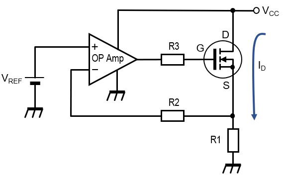
Figure 4. Constant current circuit using an operational amplifier
ID flows when a positive voltage VGS is applied to the gate of the MOSFET. When ID flows, the voltage shown in equation (1) occurs across the shunt resistor (R1).
VR1 = R1 × ID ----- (1)
Input the voltage VR1 generated by R1 to the inverting terminal (-) of the operational amplifier. On the other hand, the reference voltage is input to the non-inverting input terminal (+). Let this voltage be VREF. As mentioned earlier, the operational amplifier has an imaginary short circuit operation, so the inverting input terminal (-) has the same voltage as the voltage (VREF) of the non-inverting input terminal (+). Therefore, the following equation (2) holds between the voltage across R1 (VR1) and the reference voltage (VREF).
VREF = R1 × ID ----- (2)
Equation (3) holds from equations (1) and (2).
VR1= VREF ----- (3)
In other words, VR1 is determined by the reference voltage. The fact that VR1 is determined means that if the shunt resistor (R1) value is fixed, the ID will inevitably be determined.
Verification of constant current circuit built into 20A electronic load device
It was stated that the ID is determined when VREF and R1 are determined from the relationship of equation (3). Here, Figure 5 below shows only the constant current circuit part extracted from the circuit diagram in Figure 2.
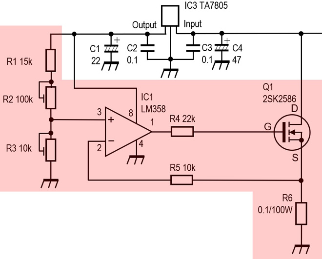
Figure 5. Constant current circuit of a 20A electronic load device
The specifications of this electronic DC load device are set so that a maximum of 20 A can flow. The shunt resistor (R6) inserted between the source and ground of the MOSFET is 0.1 Ω/100 W. For example, if this is 1 Ω, the voltage VR6 across R6 is:
VR6= 1Ω × 20 A = 20 V
This calculation comes from equation (1) above. If R1 in equation (3) is replaced with R6 in the actual circuit, VR6 = VREF. From this, the reference voltage is set to 20 V, and that voltage and 20 V of VR6 are input to the (+) terminal and (-) terminal of the operational amplifier, but this is higher than the power supply voltage of the circuit. It is not suitable for configuration.
So, let's set R6 to 0.1 Ω as one-tenth of 1 Ω. Then, VR6 becomes:
VR6 = 0.1 Ω × 20 A = 2 V.
This is an appropriate voltage, so by setting VREF to 2 V, VGS can be controlled by using the operation of the imaginary short of the operational amplifier. You can automatically control the ID by increasing the VGS if the ID is low and decreasing the VGS if the ID is high.
If you want to set the ID to 1 A, find the VREF from the voltage VR6 across R6, and it will be:
VREF = 0.1 Ω × 1 A = 0.1 V.
Since the reference voltage is 0.1 V as a very small voltage, accuracy is required. Therefore, a Zener diode is often used to make the stable reference voltage, but in the circuit shown in Figure 5, a three-terminal voltage regulator is used to further stabilize the reference voltage.
As an aside, since the resistor value of R6 is 0.1 Ω and the maximum current flowing through that resistor is 20 A, the power consumed by that resistor is:
P = I2x R = 40 W.
Speaking of 40 W, it has the same amount of heat as a soldering iron. It goes without saying that a resistor or heat dissipation that can withstand this amount of heat is required.
FBDX
Technical Trivia by Dr. FB backnumber
- Generating “Sawtooth Waves” using a D/A conversion circuit and a counter IC
- Examining a D/A converter using a Resistor Ladder
- Electronic firefly and its circuit description
- Controlling the rotation speed of a DC motor
- Description of up-down counter using 74HC192 and 74HC4511 ICs
- Considerations when making a dual voltage power supply for operational amplifiers
- Observing filter characteristics with a white noise generator
- Is noise actually reduced in twisted pair cables?
- Experiments on divider circuits using a 74HC74
- Consideration of using a photocoupler as a voltage-variable resistor
- Distorted waveform spectrum as observed on a tinySA
- Trial making of a QFH antenna
- About the inductance of coils
- Operation of analog switches
- Small digital voltmeter, 2-wire type / 3-wire type. What is the difference?
- Constant current circuit using an Op-Amp
- Coaxial cable loss to UHF and SHF
- 2.4 GHz Wireless LAN Antenna
- Let’s use MOSFETS
- 25th Comparator
- The principle of PLL
- Examination of the MLA performance
- About the Fresnel zone of the SHF band
- Level difference under open and load ends of an SSG
- Is “Made in Japan” alive? (UHF adapter again)
- Possibility experiment of passive repeater with the Back-to-Back antenna
- Why you should make SWR measurements just below the antenna!
- How reliable is the L-type BNC?
- Is the Bird 43 accurate enough?
- Does a wire dipole antenna need a balun?
- Why we don’t use a silicon diode in a crystal radio?
- How to light the 7-segment LED
- Measurement of Antenna Performance on Handheld Transceivers (Part 3)
- Measurement of Antenna SWR on Handheld transceivers (Part 2)
- Measurement of Antenna SWR on Handheld transceivers(Part 1)
- An SWR meter
- V/UHF 3-Band Antenna Dismantling Note