


Technical Trivia by Dr. FB
Consideration of using a photocoupler as a voltage-variable resistor
Dr. FB
An element whose resistance changes with voltage
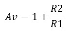
The ratio of R1 and R2 in an amplifier using an operational amplifier, shown in Figure 1, determines the voltage amplification (Av). The amplification can be continuously varied by using variable resistor values for R1 and R2. For example, when you want to automatically vary the amplification using an Arduino or similar device, it is very convenient to have a component whose resistance value changes with changes in voltage.
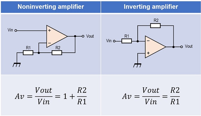
Figure 1. Calculation of the amplification gain using an operational amplifier
An FET is a component whose resistance changes with changes of voltage. Since a change in the voltage between the gate(G) and the source(S) changes the resistance between the drain(D) and source(S). It is possible to connect an FET between D and S to R1 or R2, but since FETs have three terminals, it requires some ingenuity to use them in a circuit. Therefore, I considered a 4-terminal component with completely independent input and output terminals. This can be incorporated into the amplifier circuit shown in Figure 1 above. Figure 2 shows an example of the circuit and how the component is inserted in a circuit.
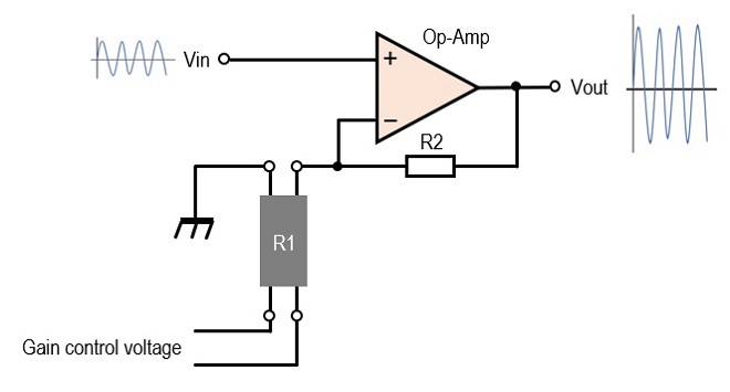
Figure 2. A circuit for adjusting the amplification gain by varying voltage
Structure of the component for changing the resistance by varying the voltage
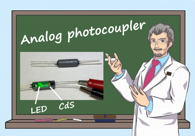
Let us consider a component other than an FET whose resistance changes with a change in voltage. A combination of a light-emitting diode (LED) and a CdS cell (CdS) could be used to achieve this characteristic, as shown in Figure 3. A CdS is a photoconductor component, and its resistance changes with the amount of light hitting the surface of the element. When light hits the surface of the cell, the resistance drops to a few kΩ drastically, and when the light is shut off, the resistance is very high, such as several MΩ or more. This light is generated by an LED and received by the CdS. Although called a voltage-variable resistor in the title, this element is generally called an analog linear photocoupler or just analog photocoupler (hereafter, photocoupler).
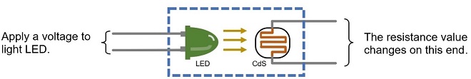
Figure 3. The structure of the photocoupler
In this component, when a voltage is applied to the input and an appropriate current is applied to the LED, the LED emits light, and the light causes the resistance of the CdS to decrease. Components with this relationship can be applied to a variety of electronic circuits. Since light is the medium between input and output, there is no electrical connection between them. Therefore, it is effective in circuits where a large degree of isolation is desired. Depending on where it is used, it may lead to a reduction in interference caused by RF feedback that plagues us in our daily lives. One point of concern is whether the input/output is linear or not, but I will investigate the characteristics through experiments.
Making the photocoupler
The structure of the photocoupler is shown in Figure 3 above. The LEDs can be of any color.
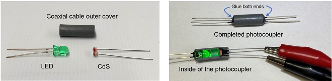
Figure 4. Fabrication of a photocoupler
Insert and glue an LED, and then a CdS in each end of a coaxial cable outer cover of about 1.5 cm in length. At this point, it is important to use black adhesive tape or black shrink tube to prevent outside light from entering the photocoupler. Figure 4 shows the completed photocoupler and its cross section cut to reveal the inside.
Photocoupler characteristics
LEDs come in a variety of light-colors and shapes. It is difficult to determine what combination is best for a photocoupler and what constitutes good characteristics.
First, a green LED and CdS are combined to make a photocoupler. The model number of the LED is not known, and the CdS is GL5537-1. It is small with a diameter of 5 mm. The experiment is to investigate the relationship between the current flowing through the LED and the resistance of the CdS mounted on its opposite side, using the connection shown in Figure 5.
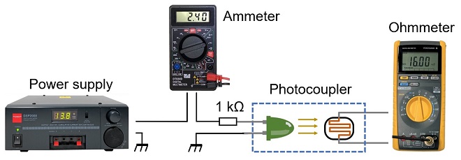
Figure 5. Experiment for the relationship between the current flowing through the LED and the resistance of the CdS
When current is applied to the LED, light is emitted inside the photocoupler, but this is a matter of concern. Figure 6 shows a photo-coupler with its cross-section cut off a little to check the internal light-emitting state.
The input-output relationship is inversely proportional, as can be seen from the above diagram. The resistance changes significantly from several MΩ to several kΩ against the current flowing from 0.1 mA to 10 mA to the LED. After the current increases to a certain degree, there is no significant change in resistance.
It is easy to see that if this photocoupler is used as R1 or R2 of the amplifier circuit shown in Figure 1, the characteristics of the photocoupler itself will be reflected in the amplification.
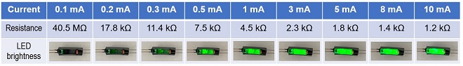
Figure 6. Inside of photocoupler
Experiment with three types of LEDs in a photocoupler
I used the green LED in the previous experiment, but I also experimented with other three types of LEDs, including blue (B) and white (W) LEDs. One of the results is shown in Figure 7, where the white LED (indicated by the orange line in Figure 7) showed a large change in resistance with the amount of current applied to the LED. The resistance value decreased significantly at higher current values for the blue (B) and green (G) LEDs. It was not clear from the experiment whether the difference in resistance value due to the difference in emission color was due to the frequency characteristics of the CdS in relation to light or to the specifications of the LEDs themselves.
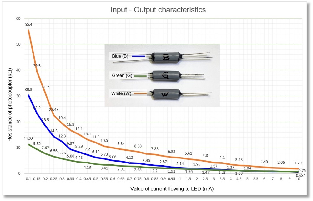
Figure 7. Photocoupler characteristics with three types of LEDs
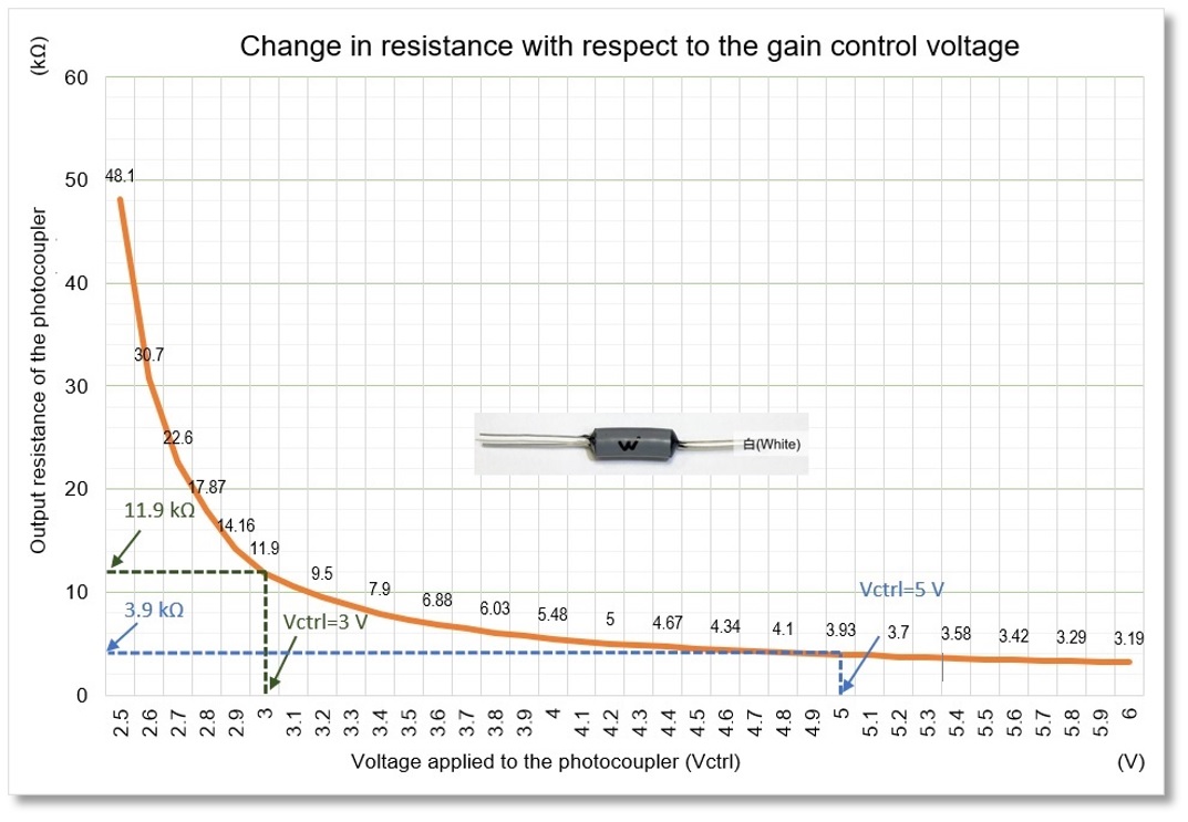
Figure 8. Change in resistance value vs. input voltage changes
Experiment using a photocoupler inserted into a real amplification circuit
The photocoupler (W) is inserted into the non-inverting amplifier circuit shown in Figure 9 to investigate the change in output level from the change in amplification (Av) due to a change in voltage (Vctrl). The photocoupler printed with a W inserted in the circuit is the white LED with the largest change in resistance with a change in current.
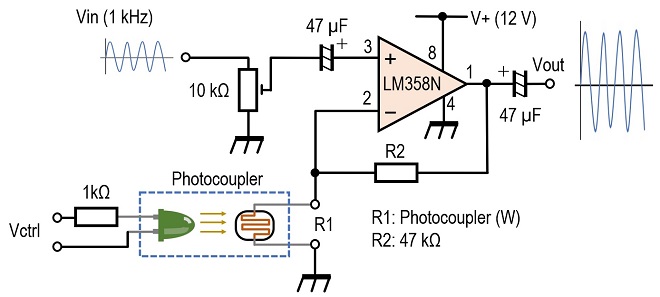
Figure 9. Investigating of changes in amplification with respect to changes in voltage
The voltage amplification of a noninverting amplifier circuit can be obtained by the following equation, as also shown in Figure 1 at the beginning of this article.
Here, R1 is the photocoupler resistor and R2 is a fixed resistor set at 47 kΩ in the experiment. There is a 1 kΩ resistor inserted in series to the LED because applying voltage directly to the LED may cause current to flow beyond specifications and it is possibly to destroy them. The maximum current to the LED is about 10 mA with this resistor.
The orange line in Figure 10 plots the output signal level when the voltage applied to the photocoupler is varied.
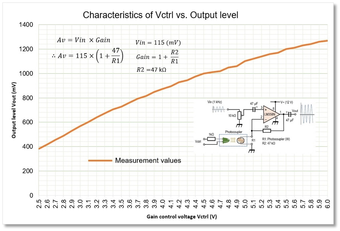
Figure 10. The characteristics of changing the output level with the gain control voltage
Verification of actual measurement values
Verify the amplification and output level of the noninverting amplifier circuit when the gain control voltage (Vctrl) is 3 V from Figures 8 and 9. A 1 kHz sine wave of 115 mV is applied the input terminal (Vin) of the circuit shown in Figure 9. The resistance value R1 of the photocoupler was 11.9 kΩ as can be read from Figure 8 when Vctrl is 3 V. From these R1=11.9 kΩ, R2=47 kΩ, and the input signal level Vin=115 mV, Vout can be calculated from the formula to be 569.2 mV. The actual measured value is 568 mV as shown in Figure 11 and the calculated and measured values are almost the same.
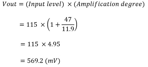
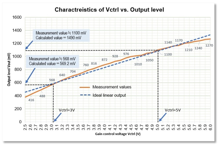
Figure 11. Difference between measured and calculated values
Let us try to verify the case when Vctrl = 5 V similarly. The resistance of the photocoupler at this time is 3.9 kΩ, as shown in Figure 8. The calculated output level is 1490 mV, while the measured value is 1100 mV. This is a large discrepancy. This is unavoidable because the change in resistance value, which determines the amplification level, is inversely proportional to y=1/ax. Nevertheless, the voltage Vctrl applied to the photocoupler in the noninverting amplifier circuit and the output level of the amplifier circuit are not perfectly linear, but the linear characteristic is close to y=ax+b, as shown in Figure 11.
Photocoupler response characteristics
A photocoupler that combines an LED and a phototransistor is similar to the LED/CdS photocoupler shown here. The light emitting element is the same as the LED, but the light receiving component is a phototransistor, so the response speed is faster. I measured the response speed of the combination of a photocoupler.
The input/output response speed of the photocoupler is shown in Figure 12. A 100 Hz square wave is input to the LED at the input leads. Observing the magnitude of the current flowing to the CdS side of the output with an oscilloscope. I found that there is a delay of 460 µs at the leading edge. The delay is around 10 µs in a photocoupler combined with a phototransistor, so this should be considered for circuits that require response speed.
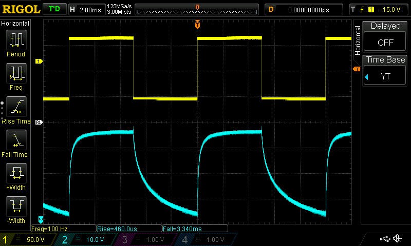
Figure 12. Response speed characteristics of a photocoupler
Summary
In this issue, I made some photocouplers that cause a change in resistance with a change in voltage and investigated its characteristics through experiments. If I have a chance, I would like to make an electronic circuit using these photocouplers.
FBDX
Technical Trivia by Dr. FB backnumber
- Generating “Sawtooth Waves” using a D/A conversion circuit and a counter IC
- Examining a D/A converter using a Resistor Ladder
- Electronic firefly and its circuit description
- Controlling the rotation speed of a DC motor
- Description of up-down counter using 74HC192 and 74HC4511 ICs
- Considerations when making a dual voltage power supply for operational amplifiers
- Observing filter characteristics with a white noise generator
- Is noise actually reduced in twisted pair cables?
- Experiments on divider circuits using a 74HC74
- Consideration of using a photocoupler as a voltage-variable resistor
- Distorted waveform spectrum as observed on a tinySA
- Trial making of a QFH antenna
- About the inductance of coils
- Operation of analog switches
- Small digital voltmeter, 2-wire type / 3-wire type. What is the difference?
- Constant current circuit using an Op-Amp
- Coaxial cable loss to UHF and SHF
- 2.4 GHz Wireless LAN Antenna
- Let’s use MOSFETS
- 25th Comparator
- The principle of PLL
- Examination of the MLA performance
- About the Fresnel zone of the SHF band
- Level difference under open and load ends of an SSG
- Is “Made in Japan” alive? (UHF adapter again)
- Possibility experiment of passive repeater with the Back-to-Back antenna
- Why you should make SWR measurements just below the antenna!
- How reliable is the L-type BNC?
- Is the Bird 43 accurate enough?
- Does a wire dipole antenna need a balun?
- Why we don’t use a silicon diode in a crystal radio?
- How to light the 7-segment LED
- Measurement of Antenna Performance on Handheld Transceivers (Part 3)
- Measurement of Antenna SWR on Handheld transceivers (Part 2)
- Measurement of Antenna SWR on Handheld transceivers(Part 1)
- An SWR meter
- V/UHF 3-Band Antenna Dismantling Note