


Technical Trivia by Dr. FB
Experiments on divider circuits using a 74HC74
Dr. FB
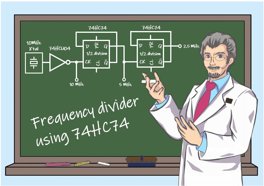
The 74HC74 is a CMOS logic IC that contains two D-type flip-flops (hereafter D-FF) in one package. I will conduct an experiment using D-FFs to create a 5 MHz and a 2.5 MHz signal from a 10MHz crystal oscillator.
What is a flip-flop?
I often see articles about flip-flop circuits when I read about electronics project. When I searched them on the Internet for the meaning of flip-flop, I found an explanation: "flip-flop means beach slippers. When you walk around in beach slippers, you hear a "flapping" sound as the beach slippers come on and off the sole of your foot, and it seems that this sound is what led people to call them “flip-flops."
Flip-flops used in electronic circuit also operate in slow motion, so that the circuit sounds exactly like a "pat-pat-pat" sound. For example, a flip-flop circuit is often used to make two LEDs alternately blink. Changing the values of R2, R3, C1, and C2 will change the blinking interval and blinking speed.
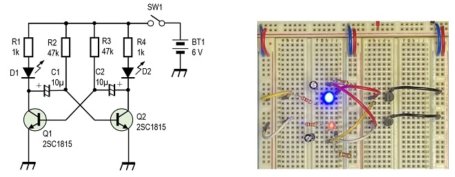 Figure 1. Circuit for alternating blinking two LEDs (Click on the breadboard to play video.)
Basic operation of the 74HC74
I will use the 74HC74 D-FF to experiment with 1/2 frequency divider circuits in this experiment. The 74HC74 has 14 pins, and Figure 2 shows the name and connection diagram of each pin.
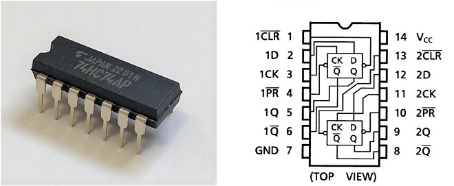
Figure 2. Appearance and pin connections of the 74HC74
The basic operation is that the state of the signal (H or L) applied to the D pin is transferred to the Q pin at the rising edge (L→H) of the clock (CK) signal. The state transferred to the Q pin is held until the next rising edge of the clock signal. Figure 3 shows these states in a timing chart. Q- (Q bar, horizontal bar above Q) outputs the inverted state of the signal appearing at the Q pin. Figure 3 shows these states in a timing chart.
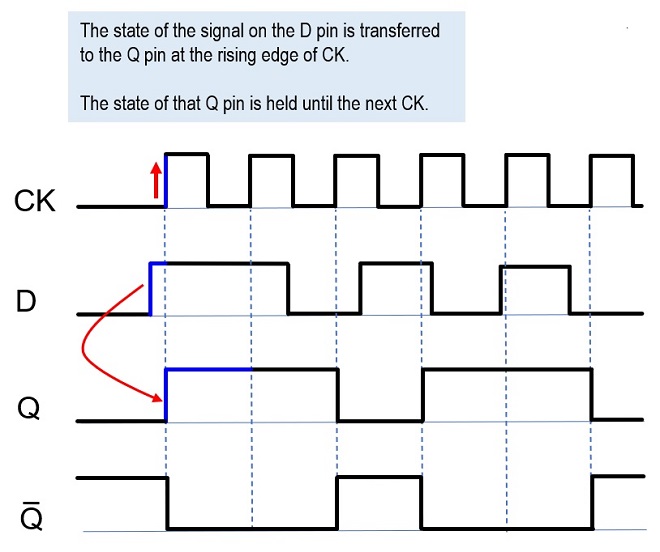
Figure 3. Timing chart of D input and Q output for clock signals
The state of the D pin is transferred to Q pin at the rising edge of the CK as you can see in the timing chart in Figure 3 above. If this D-FF is connected as shown in Figure 4, 1/2 of the clock frequency is output from the Q pin. The following is a step-by-step explanation.
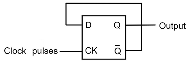
Figure 4. 1/2 Frequency divider with D-FF
Connect the Q- pin to the D pin when the D-FF is energized. The Q pin is also low level (L) because the D input pin is at L. The inverted output Q- outputs a high level (H). At the same time, the D pin goes H. When the first clock pulse is input, the H on the D pin is transferred to the Q pin at the rising edge of the clock pulse (CK). In other words, a "H" level appears on the Q pin and an "L" level is output on the Q- pin. At the same time, the D pin goes L, and on the rising edge of the next clock, L on the D pin is transferred to the Q pin. This time, the Q- pin changes to "H." Similarly, each subsequent clock cycle changes the level of the Q- pin from H to L and then from L to H.
This means that for two clock inputs (one cycle), the output of the Q or Q- pin changes only once a half cycle. This is the principle of a 1/2 frequency divider. Figure 5 shows the timing chart. The red shaded arrows indicate that the level of the Q or Q- pin changes only once during the two rising edges of CK (clock).
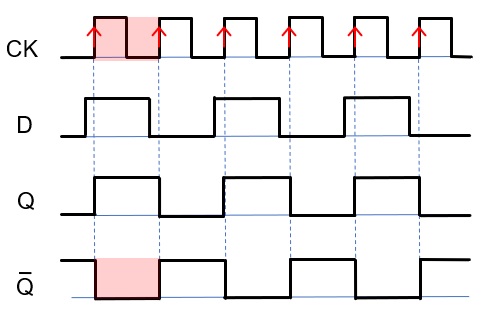
Figure 5. Timing chart showing 1/2 division by D-FF
Making a 1/2 frequency divider with D-FF
Let us try to make a 1/2 frequency divider using the 74HC74. Figure 6 shows the circuit diagram. Since it will take a time to make a 10 MHz oscillator from the beginning, I will use a crystal oscillator (unit). The output of the oscillator is converted to a square wave through a NAND gate. The rest is the D-FF 1/2 frequency divider circuit described in the previous explanations. The first D-FF divides the frequency by 1/2, and the second D-FF divides it by another 1/2. This produces 5 MHz and 2.5 MHz from 10 MHz.
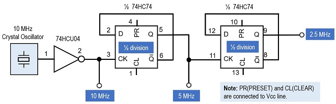
Figure 6. Experimental circuit for a 1/2 frequency divider
Figure 7 shows this circuit built on a breadboard. Since the clock frequency is as high as 10 MHz and the subsequent frequency dividers are also high frequency as RF (Radio Frequency) of 5 MHz and 2.5 MHz, signal interference occurs on the breadboard and the output signal waveform is not clean. Nevertheless, the frequency dividing can be clearly seen in Figure 8.
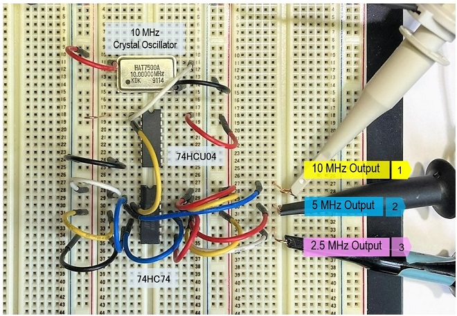
Figure 7. 1/2 frequency divider circuit built into a breadboard
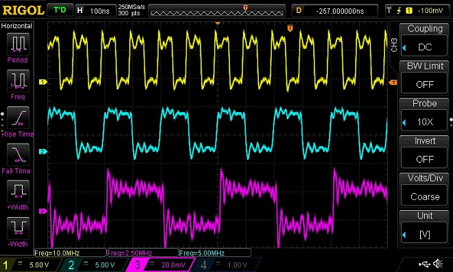
Figure 8. Comparison of output waveforms (yellow: 10 MHz, blue: 5 MHz, pink: 2.5 MHz)
Summary
I used a 74HC74 D-FF and experimented with a 1/2 divider in this issue. For example, the 74HC390 can be used to divide the frequency by 1/10. If you use two of them in succession, you can divide the frequency by 1/100, and by using several of them, you can create a 1 s. or 1 msec. time when you make a frequency counter.
FBDX
<Reference>
Connection diagram on Figure 2 is quoted from the TC74HC74 data sheet provided by TOSHIBA.
Technical Trivia by Dr. FB backnumber
- Generating “Sawtooth Waves” using a D/A conversion circuit and a counter IC
- Examining a D/A converter using a Resistor Ladder
- Electronic firefly and its circuit description
- Controlling the rotation speed of a DC motor
- Description of up-down counter using 74HC192 and 74HC4511 ICs
- Considerations when making a dual voltage power supply for operational amplifiers
- Observing filter characteristics with a white noise generator
- Is noise actually reduced in twisted pair cables?
- Experiments on divider circuits using a 74HC74
- Consideration of using a photocoupler as a voltage-variable resistor
- Distorted waveform spectrum as observed on a tinySA
- Trial making of a QFH antenna
- About the inductance of coils
- Operation of analog switches
- Small digital voltmeter, 2-wire type / 3-wire type. What is the difference?
- Constant current circuit using an Op-Amp
- Coaxial cable loss to UHF and SHF
- 2.4 GHz Wireless LAN Antenna
- Let’s use MOSFETS
- 25th Comparator
- The principle of PLL
- Examination of the MLA performance
- About the Fresnel zone of the SHF band
- Level difference under open and load ends of an SSG
- Is “Made in Japan” alive? (UHF adapter again)
- Possibility experiment of passive repeater with the Back-to-Back antenna
- Why you should make SWR measurements just below the antenna!
- How reliable is the L-type BNC?
- Is the Bird 43 accurate enough?
- Does a wire dipole antenna need a balun?
- Why we don’t use a silicon diode in a crystal radio?
- How to light the 7-segment LED
- Measurement of Antenna Performance on Handheld Transceivers (Part 3)
- Measurement of Antenna SWR on Handheld transceivers (Part 2)
- Measurement of Antenna SWR on Handheld transceivers(Part 1)
- An SWR meter
- V/UHF 3-Band Antenna Dismantling Note