


Short Break
Building a 20 Amp electronic DC load device using an N-channel MOSFET for the load
I bought a used transformer type 30 A DC regulated power supply at a flea market. Although it worked, I tried an experiment by connecting my IC-7600 to the power supply to see if it could really draw a current of 30 A. The IC-7600 is Icom's HF + 50 MHz All Mode 100 W transceiver. According to the electrical specifications of IC-7600, the maximum transmission current is stated as 23 A. The load is just right for testing this power supply.
When I connected a dummy load to the IC-7600 and started transmission with RTTY, I was able to confirm a current of less than 20 A at full power, and the power supply I purchased worked normally, and I was relieved. Next, assuming RTTY QSOs, I conducted a test in which continuous transmission for 20 seconds and reception for 20 seconds were repeated. About the 20th time, the power output suddenly stopped. When I opened the power supply cover and checked the circuit and found that a diode bridge on the secondary windings of the transformer was broken.
What is an electronic DC load?
An electronic DC load is a device used to test the performance of power supplies and batteries. The inside is composed of semiconductor elements. The load connected to the output terminal can be set electronically. The device I built this time incorporates a “Constant current circuit” that allows a constant current to flow, even if the output voltage of the power supply changes during operation. With this electronic DC load device, you can achieve what you cannot do with a resistive load.
As mentioned above, I used an IC-7600 for the performance test of the DC regulated power supply because I had no other load that could carry a large current of 20 A. Actually, it is easy if you connect a resistor, but if you try to take out 20 A from the 13.8 V DC output terminal, in addition to the 0.69 Ω resistor, you need a resistor that can consume 276 W of power from P = I2 x R. It is not easy to obtain such a resistor. Also, if you want to change the current value to be taken out, you need to change the resistance value of the load, and the resistance load is not realistic. Therefore, instead of a resistor, an electronic load that I built was connected.

Figure 1. Conceptual diagram of a resistor load and an electronic load
On the left in Figure 1 is a classic resistor load device. It is necessary to change the resistance value according to the current value to be passed. The figure on the right is a conceptual diagram of an electronic load device that uses semiconductor components. A large current is passed through the semiconductor to make it a load. By changing the current flowing through the base, the collector current can be changed, and continuous power consumption is possible.
Circuit diagram of electronic load device
The built circuit is the dotted line shown in Figure 2 below. The drain current (ID) is controlled by changing the VGS (Gate-Source voltage) of the N-channel MOSFET. The power supply for this circuit is taken from the power supply under test (regulated power supply). In other words, the current flowing from the power supply causes this MOSFET to act like a resistor and consume it as heat.

Figure 2. Circuit diagram of electronic load using MOSFET
The device has a constant current circuit installed so that ID will always be constant, even if the voltage of the regulated power supply changes. In both Figure 3 (a) and (b), the ID changes as the VGS changes. In Figure 3 (a), the VGS is changed by changing the VR to control the ID, but the ID changes unintentionally due to the voltage applied to the MOSFET, or the temperature rise of the MOSFET. Figure 3 (b) constitutes a constant current circuit in which a resistor (R) is inserted between the source and ground, and the voltage generated across the resistor is compared with the reference voltage (VREF) to obtain a constant ID. Since the reference voltage needs to be stabilized, the output voltage of the 5 V 3-terminal regulator is divided by resistors.
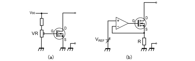
Figure 3. Principle diagram of MOSFET current control circuit
Explanation of each part
(1) Q1 (2SK2586)
Renesas Electronics' 2SK2586 N-channel MOSFET is used as the load. (Figure 4) Unfortunately, it has already been discontinued, but it seems that it is in stock in the street markets. Regardless of this part number, the drain current (ID), drain-source resistance (RDS) in the ON state, and specifications similar to the characteristic diagram shown in Figure 5 are compatible.
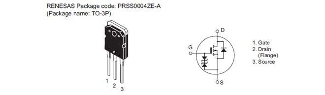
Figure 4. Terminal name of 2SK2586 (quoted from Renesas Electronics data sheet)
The ID of 2SK2586 is listed as 60 A according to the Renesas Electronics data sheet. To maintain stable performance, the maximum current of the electronic load is designed to be 20 A. Figure 5 is an excerpt from the company's data sheet, showing the relationship between drain-source voltage (VDS) and ID with respect to gate-source voltage (VGS ). The figure on the right is a processed version of the graph. It can be seen that the ID is not so much related to VDS in the green saturated region, but rather heavily dependent on VGS . For example, when VGS is 2.5 V, the ID is 10 A, and when VGS is 3 V, 40 A is flowing. In the saturation region, the ID is almost constant, even if the VDS is changed. To allow 20 A to flow through the load, the VGS can be read in the characteristic diagram as approximately 2.7 V.
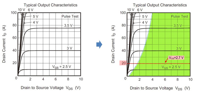
Figure 5. VDS vs. ID characteristics for VGS (quoted from Renesas Electronics data sheet)
(2) D1 (S60SC4M)
Two Schottky barrier diodes are included in one package. When connecting the positive and negative outputs of the regulated power supply to this electronic load device, it is inserted for the purpose of protecting the circuit, even if it is accidentally reversed. Any Schottky barrier diode with the same current capacity will do. This time, I used two diodes in the package connected in parallel. The reason for connecting a Schottky barrier diode to the input terminal of the power supply is that the forward voltage (VF) is as low as 0.2 V, compared to 0.6 to 0.7 V of the VF of a general PN junction diode, and the voltage drop of the regulated power supply is reduced.

Figure 6. External and internal connection diagrams of S60SC4M
(3) R6 (0.1 Ω/100 W)
The component in Figure 7 is one of key parts of this electronic load device. Since large current flows in a MOSFET, I used what is called a metal clad resistor, that can withstand the high current. The resistance value is 0.1 Ω, and the power consumption is 100 W. It is possible to pass a current of over 30 A by calculating from the resistance value and wattage, but sufficient heat dissipation is required. This metal clad resistor was attached to an 8 cm square aluminum die-cast heat sink without heat sink tape and without a cooling fan, and it was damaged when a current of about 10 A was passed for 3 minutes. This resistor is used to construct a constant current circuit that always flows a constant ID, even if the voltage of the regulated power supply changes.
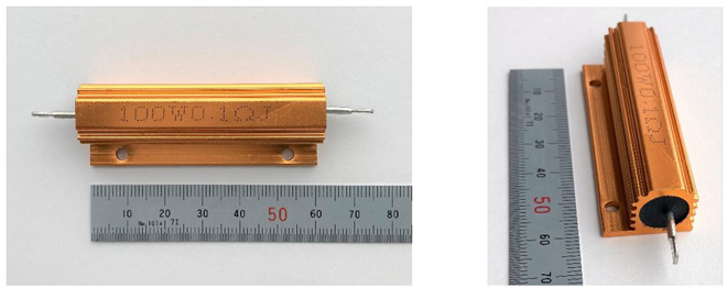
Figure 7. 0.1Ω/100W Metal Clad Resistor
(4) Voltmeter (DS1), ammeter (DS2)
DS1 and DS2 are 2-wire 3-digit digital voltage display units. The output voltage and output current of the regulated power supply are displayed digitally, and the one I purchased as a unit is used as it is. Most regulated power supplies are equipped with voltage and ammeters, so they are not absolutely necessary for this device.
The voltage display can be used as it is by connecting the red and black lead wires of the unit to the regulated power supply, but the current display requires a little ingenuity. Since it is originally a voltage display unit, the voltage generated across the 0.1 Ω/100 W resistor (R6) connected between the source and ground of MOSFET is displayed by this voltage display unit, and the display number is used as the current value. If 10 A flows through this 0.1 Ω resistor, a voltage of 1 V is generated across this resistor. In this case, if the digital voltage display unit is connected to both ends of R6, "1.00" will be displayed. Actually, 10 A is flowing, so I would like to display "10.0," but since the voltage is 1 V, it will be displayed as "1.00." When the voltage of 1 V is amplified 10 times, the voltage display can be read as the current display.
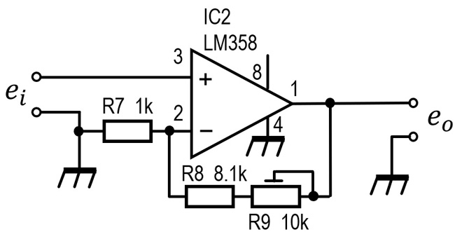
Figure 8. Circuit that increases the voltage by 10 times (20 dB)
Figure 8 shows an amplifier circuit that increases the voltage by 10 times. The original circuit is a non-inverting amplifier circuit that uses an operational amplifier. The output is fed back by R8 and R9 to have a gain. For reference, the voltage gain of this circuit can be calculated by the following equation. Adjust the gain 10 times using R9 as a variable resistor.

(5) IC1 (LM358N)
A general-purpose single-power operational amplifier. Two operational amplifiers are included in one package. IC1 is used for the constant current circuit, and IC2 constitutes the 10-times amplifier, shown in Figure 8. Since IC1 and IC2 form a circuit that is physically separated, two independent LM358s are used.
(6) FA1 (cooling fan)
The cooling fan operates at 12 V. When a large current is drawn, Q1, R6, and D1 generate a large amount of heat, so a cooling fan that can dissipate sufficient heat is required. The size of the cooling fan used in this device is 80 x 80 x 25 mm. I tried to reduce the size with a cooling fan of 80 x 80 x 15 mm, but I damaged one metal clad resistor (R6) due to insufficient air volume.
(7) Heat sink
Electronic circuits are important for assembling, but heat dissipation measures are also very important. The heat sink was finally made of 100 x 150 x 14 mm aluminum die-cast with fine fins. I conducted an experiment with 100 x 100 x 20 mm aluminum die-casting earlier, but probably because the number of fins was insufficient, the heat dissipation was unexpectedly small, and in this case as well, the metal clad resistor was destroyed.
Assembly
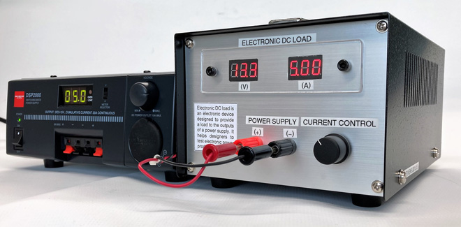
In addition to the volume knob that controls the current, the power input terminal, voltage, and current display units are attached to the front panel. I wanted to make it look cool, so I put an acrylic window board on the front of the display and used black hexagon socket screws for the mounting screws. (Figure 9)
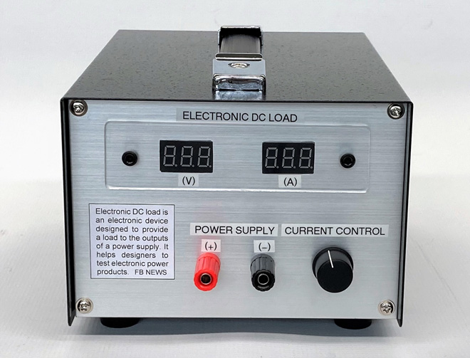
Figure 9. Front panel layout
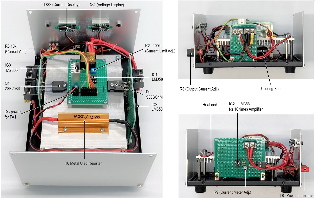
The electronic circuits are pretty simple. The constant current circuit is built onto a 50 x 70 mm glass epoxy universal substrate (Figure 10, left). Assembly that takes into consideration the heat generated from semiconductor components and resistors is essential. I used a red-black DC cable for the power supply of the radio to wire the part where a large current flows. If a thick wire is soldered to a universal board with holes, it will be difficult to handle due to wire routing, and so on, so I used a terminal block with screws, as shown in Figure 10 (right).
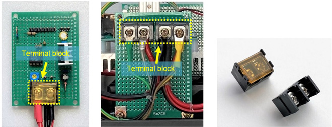
Figure 10. Components mounted on a universal board
The heat sink dissipates heat with sufficient air volume. The cooling fan is installed by sandwiching a 5 mm rubber sheet between it and the chassis. Wind noise cannot be reduced, but the rubber is effective for suppressing vibration of the cooling fan and chassis.
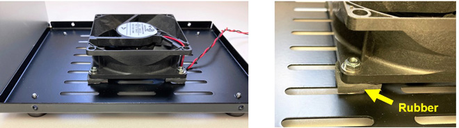
Figure 11. Installation of cooling fan
Internal structure
Cooling fans and heat sinks are often mounted on the outside of the case, but I put them inside the metal case because I didn't have a properly sized heat sink, case, and cooling fan. I was worried about insufficient cooling, but when I tried to take in the air from the bottom and let it out through the slits on the side of the case, it seems that the air flow was good. In the tests, it worked without breaking even at 20 A and 10 minutes of continuous operation. If it was a continuous operation of 10 A, it operated with a margin of 30 minutes, so you can see that the effect of air cooling has come out.
Summary
Even if you make an electronic load device, it is not a device that you often use for amateur radio operation and electronic work, but you will learn about MOSFET operation, constant current circuits, and handling of heat-generating parts.
This time, I bought a used stabilized power supply on impulse, and I wanted to test the power supply, so I made an electronic load device. The most expensive component was the metal case. It cost about 5,000 yen (approximately US 45 dollars). I wanted to make it cool, and I wanted to make it look like a commercial product, so I made it with a handle. The size of the heat sink was also very limited. I spent a lot of time designing the structure because the case would be too large to fit the heat sink, and the heat dissipation effect would be diminished if it was made smaller.
I was relieved that the metal clad resistor had a capacity of 100 W, but this is the minimum condition when it is completely attached to the heat sink, and the specification of 100 W is satisfied when it is not attached to the heat sink. I destroyed two of them during the experiment. The same applies to the MOSFET. It is important that the heat dissipation tape is firmly attached and securely screwed to the heat sink.
The most worrisome thing is the ammeter attached to the main body. The minimum measured voltage of the digital voltage display unit used this time is 2.5 V. Since the voltage across R6 is amplified 10 times and input to the digital voltage display unit, it will not reach 2.5 V unless a current of 0.25 A or more flows through R6, and the current will not be displayed below that. More ingenuity is needed here.
CL
Technical data sheet provided by Renesas Electronics Corporation (Japan)
Cooperation: Tachibana Electronic Solutions Co., Ltd.
Short Break backnumber
- How many colors do you see when a colored disc is rotated at high speed?
- Making a dual Positive/Negative voltage power supply in a single box, for experiments
- Building of an RF Volt-Ammeter for QRP operation
- White noise generator project
- One day electronics project – Making a simple antenna tuner for QRP operations
- Can the RHM12 portable antenna be matched with a bicycle body on HF?
- Making an “ON AIR” lamp using LM358
- Making a simple anemometer
- Making a sound machine say “Good morning. Thank you for everything.”
- Electronics project for the 10 MHz reference signal generator (2)
- Electronics project for the 10 MHz reference signal generator (1)
- Making a straight type AM radio using a TA7642 IC
- About splitters
- Electronics project for FB NEWS: Making a decoration light string
- Making a Simple Electric Field Strength Meter
- Building a simple QRP power meter
- Building a 20 Amp electronic DC load device using an N-channel MOSFET for the load
- Building an automatic backup power switching unit
- Overvoltage protection device using LM358: Part 2
- Building an Over Voltage Protector: Part 1
- Making a 50 MHz monoband MLA without a variable capacitor
- Making a 50 MHz monoband MLA.
- Let's connect a computer headset to the IC-705
- Building a microphone selector
- Building an audio amplifier using an LM386 IC chip
- An External Keypad for Icom Transceivers
- After all, is the receiver good for Up-conversion?
- Find the gain of the stack antenna
- The mystery of controlling the microphone and PTT with only two wires
- RFID tag